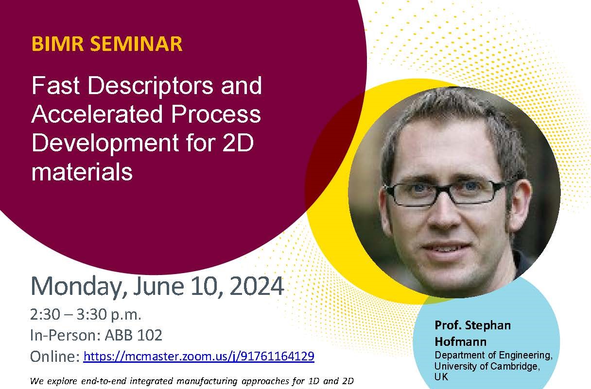
Fast Descriptors and Accelerated Process Development for 2D materials
Jun 10, 2024
2:30PM to 3:30PM

Date/Time
Date(s) - 10/06/2024
2:30 pm - 3:30 pm
Categories
Stephan Hofmann
Department of Engineering, University of Cambridge, UK
We explore end-to-end integrated manufacturing approaches for 1D and 2D nanomaterials and their technological potential ranging from digital bio-nano-analytics [1] to non-volatile memories [2,3] and machine learning accelerators. [4] For much-needed accelerated materials development, there is demand for characterisation approaches that can both resolve complex structure-property relations down to the atomic detail [5] as well as enable smart, high throughput screening.[6,7] This talk will focus on our cross-correlative operando and high-throughput approaches for exploring nucleation, crystal growth and process mechanisms for thin films and 2D materials at the atomic monolayer limit using CVD-based approaches coupled to new process vectors such as catalytic enhancement.[8,9]
Using a Kramers-Kronig constrained variational fitting algorithm for imaging spectroscopic imaging ellipsometry (SIE) we demonstrate non-destructive, efficient characterisation and scalable mapping of multi-layer semiconductor heterostructures with 1 ?m lateral resolution. We demonstrate operando capability for thermal HfS2 oxidation up to 400?C, providing insights into the temperature and time dependent nature of self-limiting oxide growth, as well as the trapping and eventual release of sulfur reaction products. We show that planar imaging with conventional SEM can give a very strong secondary electron contrast between prevalent van-der-Waals epitaxial orientational alignments as well as non-epitaxial mono-layer h-BN domains deposited on Ni(111), thereby opening powerful orientational and film texture mapping capabilities. We demonstrate how this can be used to systematically explore mono- and bi-layer h-BN film texture evolution, from isolated domain nucleation to full coverage, including the resulting domain boundary structures. We also demonstrate high-throughput operando SEM to directly interrogate the mechanisms of catalytic 2D formation including salt-assisted WS2 layer CVD. We thereby employ increasingly automated, machine-learning assisted analysis and parameter space exploration.
References
[1] Hexagonfab.com
[2] Pinquemal-Banci et al., Nat Comm. 11, 5670 (2020).
[3] Tappertzhofen et al, Nanoscale 9, 17494 (2017).
[4] Tye et al. Nature Electronics, 6 , 479 (2023).
[5] Schmitt et al. Nature, 608 , 499, 2022.
[6] Potocnik et al. Nano Lett., 23 , 5506, 2023.
[7] Burton et al. ACS Nano, 17 , 1229, 2022.
[8] Hofmann et al. J. Phys. Chem. Lett., 6 , 2714, 2015.
[9] Wang et al. ACS Nano, 13 , 2114, 2019.
Bio sketch:
Stephan Hofmann is Professor of Nanotechnology at the Department of Engineering at Cambridge University, and Director of the NanoDTC Doctoral Training Centre in Nanotechnology (www.nanodtc.cam.ac.uk). His research group (hofmann-group.eng.cam.ac.uk) works on the application driven exploration of new device materials, bridging from fundamental discovery and characterisation of properties to functional device integration and manufacturing pathways. He graduated in Physics at the Technische Universita?t Mu?nchen and obtained his Ph.D. at the University of Cambridge. Prior to his faculty position, he held a Dorothy Hodgkin Fellowship by the Royal Society and a Research Fellowship at Peterhouse, Cambridge, where he is currently a Fellow.
In-Person: ABB 102
Online: https://mcmaster.zoom.us/j/91761164129
Meeting ID: 917 6116 4129
Passcode: 003687

